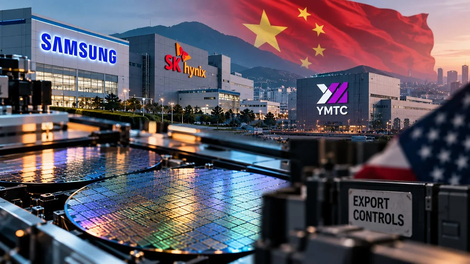
Samsung Electronics and SK Hynix are modernizing their factories in China to produce more advanced NAND memory chips, amid the growth of local competition and demand for storage in artificial intelligence data centers. The projects were revealed by Reuters this Wednesday (21), based on information from four people familiar with the plans.
Samsung is working to adopt 286-layer NAND memories at its Xian unit, responsible for approximately 40% of the company's global production of this type of chip. Currently, the factory uses processes with about 200 layers.
The initiative, internally named Monami, is expected to reach a monthly production of 5,000 wafers in December 2026, reaching 40,000 in December 2027, according to one of the sources consulted by the agency. These targets were not publicly confirmed by the manufacturer.
Samsung confirmed the modernization and stated that the changes follow United States export rules. According to the company, the goal is to meet the growing demand from international customers, including American ones, without expanding total production capacity or building new facilities.
SK Hynix is also upgrading its factory in Dalian, acquired from Intel in 2021. Three sources indicated that the company plans to migrate from the current 192-layer technology to 240-layer or higher NAND memories.
The manufacturer confirmed the installation of equipment at the unit, in consultation with the US government, but did not officially disclose the specifications of the new processes.
The number of layers is an important indicator of the evolution of NAND memory, used in smartphones, computers and SSD drives. Stacking more storage cells makes it possible to increase chip density and reduce the cost per stored capacity.
YMTC overtakes Samsung in China as US licenses restrict modernizations
The advance of the Chinese company Yangtze Memory Technologies (YMTC) adds competitive pressure to South Korean investments.
Data from the consultancy Omdia, released by Reuters, show that YMTC reached 38.5% of the Chinese NAND market in the second quarter of 2026, up from the 28% recorded in 2025 as a whole.
In the same survey, Samsung's share fell from 36% to 33.5%, while SK Hynix went from 20% to 17%. The comparison uses the annual results for 2025 and the data for a specific quarter of 2026.
YMTC is also advancing technologically. Although its portfolio consists mainly of 160- and 232-layer memories, the manufacturer already produces limited quantities of 294-layer chips and plans to develop products that exceed 300 layers, according to industry sources heard by the agency.
The South Korean companies face, however, regulatory restrictions that make it difficult to upgrade their Chinese facilities.
Since the end of the previous special authorizations, at the end of 2025, Samsung and SK Hynix need annual licenses from the United States to import certain American equipment used in semiconductor manufacturing.
The Bureau of Industry and Security (BIS), an agency of the US Department of Commerce, stated in 2025 that it intended to allow existing operations to continue, but not to authorize capacity expansions or technology upgrades at these factories.
Reuters was unable to determine the extent of the licenses already granted for the announced projects. The regulator also did not individually clarify the status of the authorizations requested by the two manufacturers.
In the case of SK Hynix, one of the sources said that the company already has authorization to manufacture chips of up to 240 layers in Dalian and may request additional permission to research technologies above 300 layers. This possibility does not yet represent an approval or a commitment to commercial production.